
Page 31 - Vol.14
P. 31
Tech
Notes
技術專文
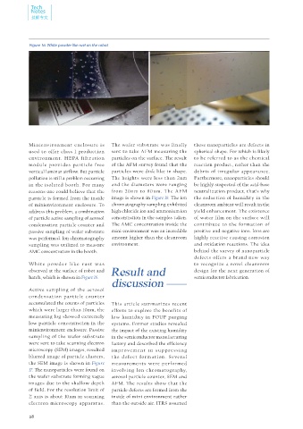
Figure 16. White powder like rust on the robot Figure 17. SEM images of nanoparticles
25.3 nm
Minienvironment enclosure is The wafer substrate was finally these nanoparticles are defects in
Acc.V Spot Magn WD 1 μm
used to offer class 1 production sent to take AFM measuring the spherical shape. For which is likely 10.0 kV 3.0 80000x 4.5
environment. HEPA filtration particles on the surface. The result to be referred to as the chemical
module provides particle free of the AFM survey found that the reaction product, rather than the
vertical laminar airflow. But particle particles were disk like in shape. debris of irregular appearance. Figure 18. AFM images of nanoparticles
pollution is still a problem occurring The heights were less than 2nm Furthermore, nanoparticles should
in the isolated booth. For many and the diameters were ranging be highly suspected of the acid-base Z [μm]
reasons one could believe that the from 20nm to 80nm. The AFM neutralization product, that’s why 1.5 References
particle is formed from the inside image is shown in Figure 18. The ion the reduction of humidity in the [1] Michael Lercel,Solving the
of minienvironment enclosure. To chromatography sampling exhibited cleanroom ambient will result in the nanodefectivity problem,
address this problem, a combination high chloride ion and ammonium ion yield enhancement. The existence 1.0 SEMATECH,November 2012
of particle active sampling of aerosol concentration in the samples taken. of water film on the surface will [2] Larry W. Shive, Richard Blank and
Karen Lamb,Investigating the Formation
condensation particle counter and The AMC concentration inside the contribute to the formation of of Time-Dependent Haze onStored
0.5 Wafers,Micro Magazine,2001
passive sampling of wafer substrate mini-environment was an incredible positive and negative ions. Ions are [3] M . Odelius, M. Bernasconi, M.
was performed. Ion chromatography amount higher than the cleanroom highly reactive causing corrosion Parrinello,Two Dimensional Ice
sampling was utilized to measure environment. and oxidation reactions. The idea Width 47.1nm Adsorbed on Mica Surface,Physical
0.0 Height 1.82nm Review Letters,78,2855,1997.
AMC concentration in the booth. behind the survey of nanoparticle [4] Lei Xu, Anna Lio, Jun Hu, D. Frank
defects offers a brand new way Y [μm] Ogletree, and MiquelSalmeron,Wetting
Wh ite p owd e r l i ke r ust wa s to recognize a novel cleanroom and Capillary Phenomena of Water on
-0.5 Mica,The Journal of Physical Chemistry
observed at the surface of robot and Result and design for the next generation of B, 1998, 102, 540-548
hatch, which is shown in Figure 16. semiconductor fabrication. [5] Peigen Cao, KeXu,Joseph O. Varghese,
discussion -1.0 Width 35.3nm and James R. Heath,The Microscopic
Structure of Adsorbed Water on
Active sampling of the aerosol Height 1.48nm HydrophobicSurfaces under Ambient
condensation particle counter Conditions,Nano Letters,2011
[6] U . B altenspergera. Real-time
accumulated the counts of particles This article summarizes recent -1.5 characterization of ultrafine and
which were larger than 10nm, the efforts to explore the benefits of -1.5 -1.0 -0.5 0 0.5 1.0 1.5 accumulation mode particles in ambient
X [μm] combustion aerosols.Journal of aerosol
measuring log showed extremely low humidity in FOUP purging science 33 (2002) 1139–1154.
low particle concentration in the systems. Former studies revealed [7] Shou-Nan Li1, Hui-Ya Shih, Shaw-Yi
minienvironment enclosure. Passive the impact of the existing humidity Yen, Jean Yang, Case Study of Micro-
sampling of the wafer substrate in the semiconductor manufacturing Contamination Control,Aerosol and
Air Quality Research, Vol. 7, No. 3, pp.
were sent to take scanning electron factory and described the effi ciency 432-442, 2007.
microscopy (SEM) images, resulted i mprove me nt i n suppre ssi n g [8] YitingKuo, Howard Tsao, TuungLuoh,
Ling-WuYang, Tahone Yang, Kuang-
blurred image of particle clusters, the defect for mation. Severa l Chao Chen, andChih-Yuan Lu, "FOUP
the SEM image is shown in Figure measurements were performed Environment Control andCondense
Reduction", e-Manufacturing &
17. The nanoparticles were found on involving Ion chromatography, DesignCollaboration Symposium 2012.
the wafer substrate forming vague aerosol particle counter, SEM and [9] Tzu-Sou Chuang, Luh-Maan Chang,
To Mitigate Airborne Molecular
images due to the shallow depth AFM. The results show that the
Contamination through Ultra-pure Air
of field. For the resolution limit of particle defects are formed from the System, Building and Environment, Vol.
Z axis is about 10nm in scanning inside of mini environment rather 59, January 2013, pp.153-163.
electron microscopy apparatus. than the outside air. ITRS assumed
28 NEW FAB JOURNAL JUNE 2014 29