Page 25 - Vol.14
P. 25

Tech
             Notes
             技術專文
                               Influence of Clean-                                                                                      Figure 1.  Critical defect trend of EUV mask   Figure 2.  Defects image on EUV mask


         room Ambient Humidity                                                                                                              35                 EUV masks defects-ITRS                                      5.00
                                                                                                                                            30
                                                                                                                                                               EUV mask inspection (Suppliers)
                                                                                                                                            25
                                                                                                                                                                                                                           4.00
                           on the Formation of                                                                                             Defect size [nm]  20                                                            2.00

                                                                                                                                            15
                                                                                                                                            10
                                                      Nanoparticles                                                                          5 0


                                                                                                                                               30
                                                                                                                                                          20
                                                                                                                                                           Flash Half Pitch [nm] 10  0      0       2.00      4.00      6.00  0  μm
               文│郭啟文│廠務技術發展專案│


               ೌྡྷ܃ᐑྤ᐀ܓ࿁׵
                                                                                                                                        Introduction                   specified limits. The level to   With the application of an AFM
               քϷ୐ɿϮݑ͛ϓٙᅂᚤ                                                                                                                                             which these contaminations need   image survey, these defects show
                                                                                                                                                                                                      a random distribution with a
                                                                                                                                                                       to be removed depends upon
                                                                                                                                        The prevailing cleanroom standard   the manufacture exquisite level   localized high density particle
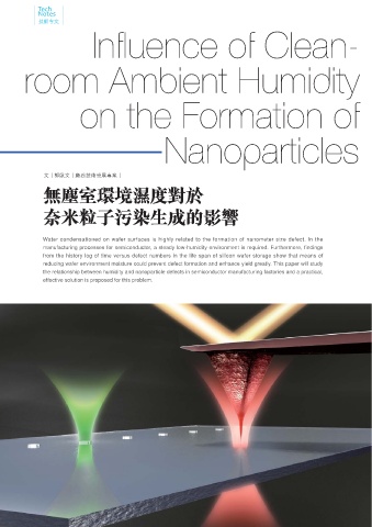
               Water condensationed on wafer surfaces is highly related to the formation of nanometer size defect. In the               is the Federal Standard 209E which   required. There are many ways   region, ty pica l ly 5-25nm in
               manufacturing processes for semiconductor, a steady low-humidity environment is required. Furthermore, fi ndings          is a document that establishes   to control contamination of the   height and less than 500nm in
               from the history log of time versus defect numbers in the life span of silicon wafer storage show that means of          standard classes of air cleanliness   production, ambient humidity,   plane diameter, and these defects
               reducing wafer environment moisture could prevent defect formation and enhance yield greatly. This paper will study      for airborne particulate levels in   pressure, temperature, particle   could  easily be removed by water
               the relationship between humidity and nanoparticle defects in semiconductor manufacturing factories and a practical,     cleanrooms and clean zones, but   filtration, chemical filtration and   rinsing or heat treatment. It
               effective solution is proposed for this problem.                                                                         there is  more and more evidence   air flow directions  all need to be   appears that the time dependent
                                                                                                                                        showing nanoparticles will be   tightly restricted.           ha ze may be approx i mately
                                                                                                                                        the issue presenting an enormous                              close to the water spot. The
                                                                                                                                        challenge to N10 and N7 production   Si l icon wa fe r s  a r e us e d  to   water adsorption on the wafer
                                                                                                                                        in the semiconductor industry.   transfer patterns on the surface   surface is due to the existence of
                                                                                                                                        Particle defects which have a  size   of the wafers. The fabrication of   ambient moisture which is very
                                                                                                                                        of less than 20nm were usually   semiconductor circuits requires   adhesive to the airborne molecular
                                                                                                                                        detected on the EUV mask[1]. The   multiple pattern layers, thus   contaminations. This is the main
                                                                                                                                        trend chart and the AFM image   anything that is not intended   speculation to the flat dish shape
                                                                                                                                        of particle defect on the EUV   to be deposited on the wafer   and high hydrosoluble properties
                                                                                                                                        mask are shown in Figure 1 and   surface is regarded as defect. For   of the defects. Larry W. Shive et al.
                                                                                                                                        Figure 2. Besides, nanoparticles are   example, the “time-dependent   performed a series of wafer storage
                                                                                                                                        atomic force dominated defects   haze” (TDH). TDH is a formation   contamination studies. Dummy
                                                                                                                                        which are difficult to remove,   of light point defects which  were   wafers were immediately packaged
                                                                                                                                        different to the microparticle   not present when the bare wafers   for 6 and 18 months after thorough
                                                                                                                                                                                                                             [2]
                                                                                                                                        forces. With i n a cont rol led   just left the production line in the   clean and defect inspection . The
                                                                                                                                        environment, the concentration of   manufacturing factory. The “time-  trend chart of the wafer defect size
                                                                                                                                        airborne molecular contamination   dependent haze” is shown in Figure   larger than 0.12um after 6 month
                                                                                                                                        and particles are controlled to   3.                          and 18 month storage is shown in


                                                                                                                                                                                                              進入台積兩年餘,學習奈米粒子
                                                                                                                                                                                                           啟文
                                                                                                                                                                                                              污染防治的相關知識,很感謝長
                                                                                                                                                                                                              官與同仁一路來的支持與協助,
                                                                                                                                                                                                              提供我成長與修習的機會。
                                                                                                                                                                                                         郭 Chi-Wen Kuo


             22                                                                                                                                                                                                 NEW FAB JOURNAL         JUNE 2014  23
   20   21   22   23   24   25   26   27   28   29   30