
Page 73 - Vol.13
P. 73
laser sensor to an image camera. The
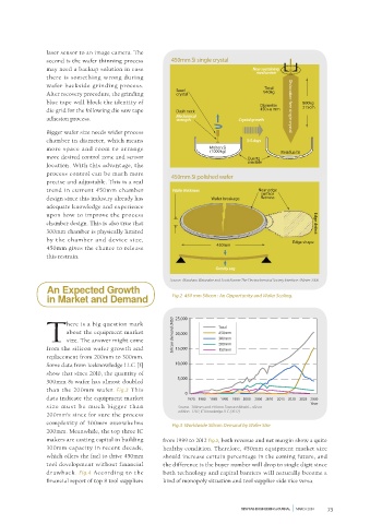
second is the wafer thinning process 450mm Si single crystal
may need a backup solution in case New sustaining
mechanism
there is something wrong during
wafer backside grinding process.
Seed Total
After recovery procedure, the grinding crystal 940kg
blue tape will block the identity of 800kg
Diameter Dislocation-free single crystal
die grid for the following die saw tape Dash neck 450+α mm 215cm
Mechanical
adhesion process. strength Crystal growth
Bigger wafer size needs wider process
chamber in diameter, which means 3-5 days
more space and room to arrange Molten Si Residual Si
(1000kg)
more desired control zone and sensor Quartz
location. With this advantage, the crucible
process control can be much more 450mm Si polished wafer
precise and adjustable. This is a real
trend in current 450mm chamber Wafer thickness Near edge
surface
design since this industry already has Wafer breakage atness
adequate knowledge and experience
upon how to improve the process
chamber design. This is also true that Edge defect
300mm chamber is physically limited
by the chamber and device size, Edge shape
450mm
450mm gives the chance to release
this restrain.
Gravity sag
Source. Masaharu Watanabe and Scott Kramer The Electrochemical Society Interface • Winter 2006
An Expected Growth
in Market and Demand Fig.2 450 mm Silicon : An Opportunity and Wafer Scaling.
here is a big question mark 25,000 Total
about the equipment market Silicon demand (MSI) 20,000 450mm
Tsize. The answer might come 300mm
200mm
from the silicon wafer growth and 15,000 150mm
replacement from 200mm to 300mm.
Some data from Iceknowledge LLC [3] 10,000
show that since 2010, the quantity of
5,000
300mm Si wafer has almost doubled
than the 200mm wafer. Fig.3 This
0
data indicate the equipment market 1975 1980 1985 1990 1995 2000 2005 2010 2015 2020 2025 2030
Year
size must be much bigger than Source. 300mm and 450mm Forecast Model – silicon
edition -1202, IC Knowledge LLC (2012)
200mm’s since for sure the process
complexity of 300mm overwhelms Fig.3 Worldwide Silicon Demand by Wafer Size
200mm. Meanwhile, the top three IC
makers are casting capital in building from 1999 to 2012 Fig.5, both revenue and net margin show a quite
300mm capacity in recent decade, healthy condition. Therefore, 450mm equipment market size
which offers the fuel to drive 450mm should increase certain percentage in the coming future, and
tool development without financial the difference is the buyer number will drop to single digit since
drawback. Fig.4 According to the both technology and capital barriers will naturally become a
financial report of top 8 tool suppliers kind of monopoly situation and tool supplier side vice versa.
NEW FAB ENGINEERING JOURNAL MARCH 2014 73