摘要
十八吋的挑戰 創新與新奇

New market demand from sort of mobile applications upon ultra-low power devices will induce advanced technology demands, which might need 450mm silicon manufacturing technologies to drive low cost and high volume production availability. Since there are not obvious differences on process materials and methods in comparison with 300mm technology, the advantage of developing 450mm technology is integrated with more adequate chamber space and brand new designs to enhance process control capability and overcome those burden or limitation in 300mm’s.
Go or No go that is the Question
It seems like a military operation waiting the D day’s coming for the whole industry to be devoted to a brand new era. We do believe there is no main technical blockage on the way to create this new world. It is true that all kind of materials and methodologies are almost ready sine both 300mm and 450mm processes share with the same technology node. Therefore, more die-cost saving will finally become the fatal weapon to win the survival. For sure, an oligopoly in tool demand side makes tool supply side become hesitated due to the concerns of tool market in total quantity. In this article, some analyses might give a hint whether the “operation” should be Go or No go.
Physical Limitations from the Earth
Daydreamers always think where is the best location for human beings to extend the wafer size perfectly with the lowest cost. The answer might be the Moon since there is only 1/6 of the Earth’s gravity to prepare colossal size silicon ingot without concerns from the sag in the wafer center. Si wafer thickness can be shrunk to the thinnest level, which means wafer intrinsic cost could be much lower. Besides, heavy tool parts can be easily handled manually without sophisticated design assistant tools like lifters or cranes. Furthermore, it is also possible to get bigger lens size to improve the throughput of photography tools.
A vacuum environment in the Moon also benefits to grasp eUV (Extreme ultraviolet) from the Sun without concerning power consumption for the extremely high power laser source. The vacuum environment can also help to avoid extra oxidation as wafers transferred to the next process step. Due to less weight in the Moon, less cooling capacity can be gained from the lithography exposure stage for air floating or magnetic floating movement.
Return to the Earth and back to the real world, the industry encounters so many challenges not just coming from gravity. Therefore, plenty of innovations are necessary to put 450mm era into practice.
Discovery of New Markets and Demands
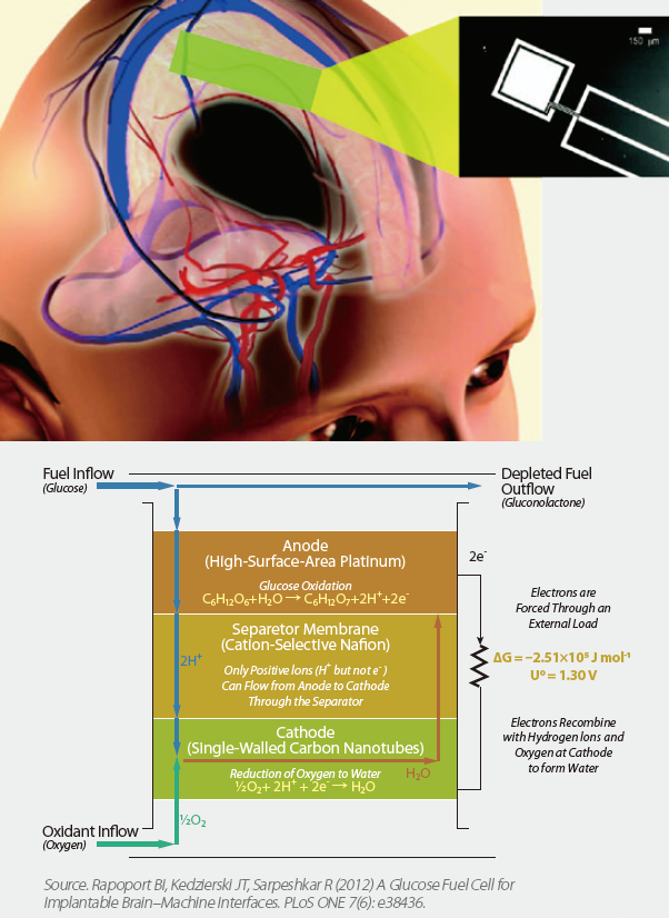
First of all, what are the expectations from this industry upon 450mm era? Of course, economic factor is the most fundamental consideration for more production output with more die cost saving. Tool supplier side also gives hope upon the new market demand from not only mobile demands but also from human health caring demands. In 2012, MIT (Massachusetts Institute of Technology) has announced a novel glucose fuel cell, development work granted by NIH (National Institute of Health) and Office of Naval Research, which is manufactured by semiconductor process, to utilize blood sugar to generate electricity as bioimplantable power sources. Fig.1 [1] This indicates ultra-low power chips or micro-devices can be implanted in human body and operated in a very long period time without changing battery because this kind of glucose fuel cell can support electricity successfully.
Fig.1 Power Extraction from Cerebrospinal Fluid by an Implantable Glucose Fuel Cell.
Those ultra-low power consumption and high computing performance devices will dominate the potential market demands in the coming decade. Beside of mobile phones, for example, new devices for wearable technology are soaring up in wider and wider applications. This stands for more advanced technology nodes which will be required soon with higher and higher die cost and more and more sophisticated manufacturing difficulties.
450mm era brings an opportunity to lower the cost and technical barrier by new design chamber, IT technology and advanced process control. In 90nm technology node, the mask layers are below forty, but it will become around seventies in 10nm technology node. It seems impossible to drive the ultra-low power application become poplar without aggressive die cost saving and more output production.
Weakness and Strength
Based on conservative estimation, even by shot or scan process cannot provide double throughput capability, the die cost saving still can reach around 20% in comparison with same technology node in 300mm production.
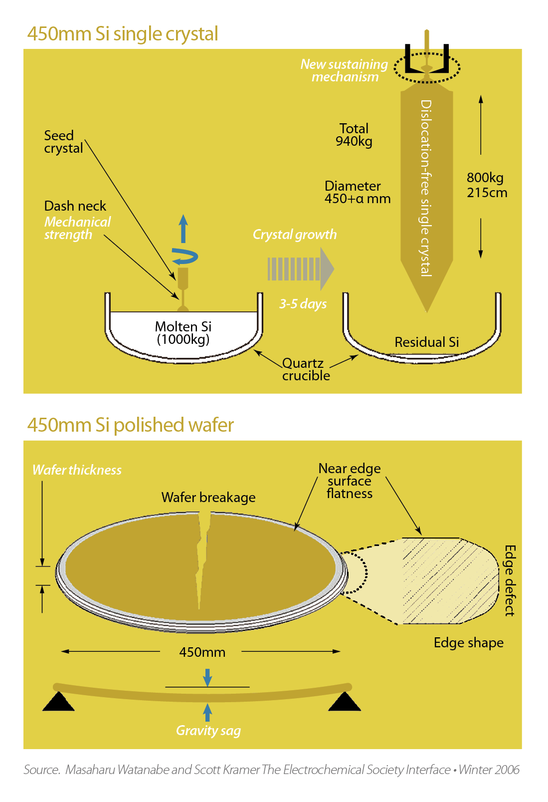
Silicon wafers are made by CZ method (Czochralski method), followed 300mm’s, in 450mm era. Fig.2 The main issue is the center sag level worse than 300mm’s. If the sag level needs to keep as 300mm’s level, the wafer thickness will reach 1744um, far thicker than current standard 925 +/- 25um. [2] The potential impacts are wafer handling and the silicon defects appearance after high-temperature thermal treatments. The other challenge is the silicon ingot might be hardly to reach the same length like 300mm’s. Shorter ingot length, thicker wafer and longer crystallization and cooling time indicate the cost reduction will take more innovations and longer learning curve to reach.
Fig.2 450 mm Silicon : An Opportunity and Wafer Scaling
This industry has got a consensus on making a standard to remove wafer notch, which is replaced by 3 wafer back-side fiducial marks away from wafer bevel 1.5mm. It is not so complex to set up a brand new process flow for notchless wafer production, just adjusting few steps and sequence. The benefits cover almost all kind of processes, mainly on uniformity improvements, and the hardware design of process tools can be more easier without a dedicated care on the notch area. Currently only two module need to design new solutions to meet notchless wafer characteristics. The first one is the wafer orientator or aligner. Since current wafer sorters have applied image technologies to recognize characters or patterns, therefore just a change from a pure laser sensor to an image camera. The second is the wafer thinning process may need a backup solution in case there is something wrong during wafer backside grinding process. After recovery procedure, the grinding blue tape will block the identity of die grid for the following die saw tape adhesion process.
Bigger wafer size needs wider process chamber in diameter, which means more space and room to arrange more desired control zone and sensor location. With this advantage, the process control can be much more precise and adjustable. This is a real trend in current 450mm chamber design since this industry already has adequate knowledge and experience upon how to improve the process chamber design. This is also true that 300mm chamber is physically limited by the chamber and device size, 450mm gives the chance to release this restrain.
An Expected Growth in Market and Demand
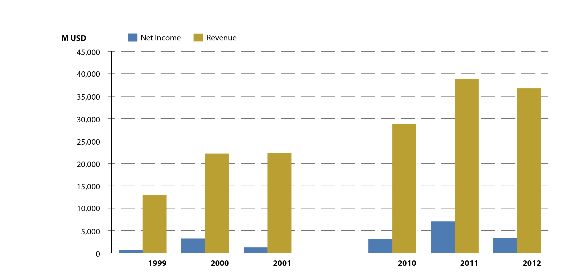
There is a big question mark about the equipment market size. The answer might come from the silicon wafer growth and replacement from 200mm to 300mm. Some data from Iceknowledge LLC [3] show that since 2010, the quantity of 300mm Si wafer has almost doubled than the 200mm wafer. Fig.3 This data indicate the equipment market size must be much bigger than 200mm’s since for sure the process complexity of 300mm overwhelms 200mm. Meanwhile, the top three IC makers are casting capital in building 300mm capacity in recent decade, which offers the fuel to drive 450mm tool development without financial drawback. Fig.4 According to the financial report of top 8 tool suppliers from 1999 to 2012 Fig.5, both revenue and net margin show a quite healthy condition. Therefore, 450mm equipment market size should increase certain percentage in the coming future, and the difference is the buyer number will drop to single digit since both technology and capital barriers will naturally become a kind of monopoly situation and tool supplier side vice versa.
Fig.3 Worldwide Silicon Demand by Wafer Size
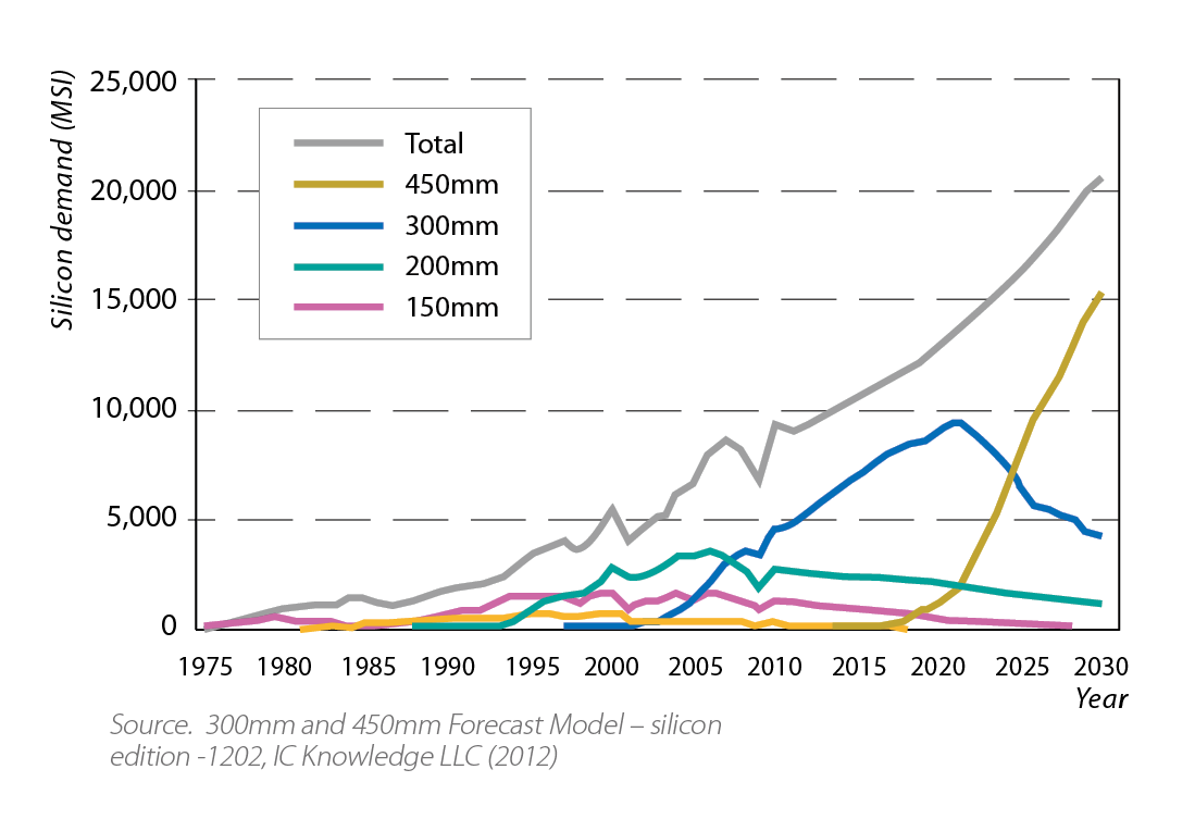
Fig.4 Tool supplier revenue and net margin (%) trend chart from 1999 to 2012
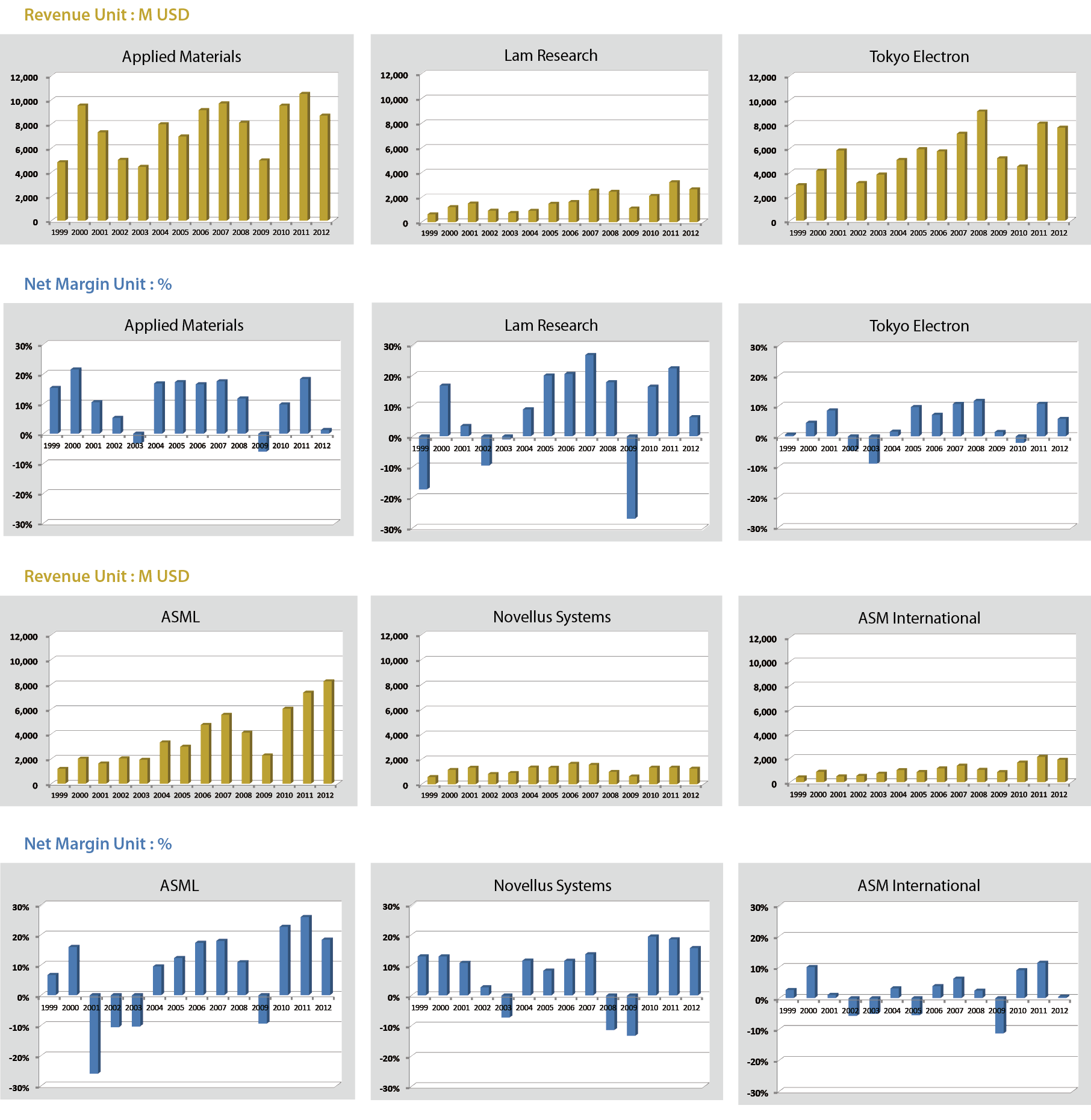
Fig.5 Top 8 tool suppliers’ net income and revenue comparison between 1999 to 2001 and 2010 to 2012.
Improvements and Innovations upon Firmware
What is the industry looking for in 450mm era? Maybe this industry could conclude as the following expectations: New equipment platform provides significant productivity improvement. Self-calibration, self-diagnostic and automatic control result in outstanding tool availability and monitor reduction. Perfect tools and hardware matching enable fast technology ramp up. Flexible module design helps mainframe cost structure. Novel Fab design drives green capability and potential. Sophisticated assisting kits prove maintenance safety and quality. Precise controls and sensors assure quality level. Smart systems enhance efficiency in production scheduling. Unique lot dispatch and planning create shorter production cycle time. Organized Big Data is applied to support excellent VM (Virtual Metrology) prediction/conjecture.
Frankly speaking, more and more manufacturing difficulties appear as the device design gets into 3D structure. The tolerance or the so-called process window has shrunk to a very narrow range. The requirements on process control become very picky than before. To achieve this, more delicate sensors arrangement and process data processing are responding in 450mm tools. Bigger process chamber size compared with 300mm’s brings the room for the installation of those sensors. Along with sensor installation, the speed of feed-back control loop is required to be more exquisite. Taking an example from metal-gate process, plenty of ALD processes are applied. The temperature control along the conducting route of precursors is very critical to impact the thickness and quality. Temperature sensors and control loops decide the survival of the process quality, which is strongly correlated to device performance.
As sampling rate increases a lot, from per second to per million second, the data-output bandwidth needs to comply with this data quantity. In addition, the time delay between commands to tool’s device responding time seems a very important clue for chamber or tool matching. Furthermore, the process related log or history, including event log and process log, needs to be collected and sent simultaneously with sensor’s data to the system like FDC (Fault Detection and Classification) for further analysis and APC (Auto Process Control) function. More aggressively, 450mm tool will include data collection from facility and sub-Fab module, like pumps, power generators, chiller or heat exchangers, local scrubbers, gas cabinets, etc., not only for green functions but also for better process control and tool device matching.
More Powerful IT Technology and Metrology
Therefore, a so-call “Organized Big Data” concept will be introduced to empower IT/AI strength. Not only just collecting data to form Big Data, but also an organized data can be usefully in time put into APC to help process control. The AI system can classify data into different priorities according to previous data-mining results. The first priority data will be processed immediately for APC or related process control system, and the lower priority data will be digested and analyzed with statistical methodologies to filter out useful correlation linkages in a separated processing system. Newly finding correlation linkages will be organized back to main system for further parallel identification and certification until adequate data quantity can answer the reliable correlations, and then this system will add those newly findings to work with main system APC or related systems. By this “Organized Big Data” concept, extracted data can become information, and the learning capability can generate more useful information. Of course, this also can help to dump really useless data to save cost on data storage.
A precise and accurate metrology also becomes more important in advanced technology node, especially below 40nm technology node. Those metrology used in Lab now have become the baseline in production line, like XRR, XRD, XRF and XPS. Integrated metrology seems one of the solutions. A common platform could integrate various solutions from different metrology suppliers. Since shorter queue time is necessary to protect process quality during inline monitor and short wavelength light source for better resolution, a vacuum measurement condition can protect the whole lot, and different kind of monitors can be completed in one platform. On the other hand, pre-layer measurement data are acquired to be calculated and improve the precision. A data feed forward system between different metrology tools is necessary for this purpose, and this system also plays a role to find out and eliminates same type tool to tool bias or mis-match.
For sure, the metrology data, including both measurement data and tool sensor data, are one of the Organized Big Data. By this, an “Advanced Virtual Metrology (AVM)” concept could be applied. In 300mm Fab, the IT infrastructure is still not healthy enough to carry out AVM due to data quality issue. “Garbage in and garbage out” is the first word as we take computer science classes. Current tool side data bandwidth and Fab backbone are not fully upgraded to optical fiber or more advanced data packet technology. At least, operation synchronization is still not set as a critical requirement in current Fab.
Optimized Manufacturing Environment
Because the critical dimension of device will come down below 100 angstrom, there is no room for extra oxidation during processes. Theoretically, Silicon can get rid of oxidation within 120 minutes as both oxygen and humidity concentration can go below 100ppm. An ultra-low oxygen and humidity environment will be built up from the beginning of 450mm Fab. Definitely, nobody will try to set up the air in the whole Fab to meet this requirement since it will be both costly and dangerous. The focus will just put on wafer transportation route to meet this ultra-low condition. Certainly, the other benefit is AMC (Airborne Molecular Contaminant) and VOCs (Volatile Organic Compounds) impacts can be lowered to some level.
Fully automation is a must for 450mm Fab operation due to the weight of each tool or device increasing a lot. In 300mm FOUP (Front Opening Unified Pod), there is a pair of handlers, but 450mm FOUP or MAC (Multiple Application Carrier) has no such a design from the very beginning. The main reason is that the empty weight of 450mm FOUP or MAC is over 20kg, which is too heavy to be handled manually and comply with related labor safety law. With a full-loaded 25 450mm wafers FOUP, the weight could be up to 25kg, even Rambo cannot handle. Although operator number will be expected to be zero in 450mm Fab, nevertheless equipment maintenance still needs engineers to cover.
Equipment engineers will encounter the same situation since over 85% parts or modules will become bigger and heavier. According to the PVD metal target supplier estimation, the weight of a PVD metal target will be around 80kg. This is really a serious issue in 450mm Fab. For wafer transportation, AMHS (Automated Material Handling System) can work on this with no doubt, but for equipment periodical maintenance upon parts and materials replacement, an assistant kit must be designed and implemented to help equipment engineers to complete their daily jobs safely.
Compact and Unique Fab Design
Since the clean room floor area is very precious, process tools are located back to back to form a working bay, which is surrounded and restrained by AMHS system. Within the working bay, there is very limited space for equipment engineers to operate, especially within tool back to back aisle, since tool length would be different as designed by different tool suppliers. Tool side by side aisle could be more luxury because chamber upper-lid may not be allowed to open in a lifted-up aside type. Therefore, it is really a dilemma in saving footprint and easy maintenance when designing the assistant kits.
As process tools get bigger and taller, Fab design will face the other dilemma. Since the total weight of AMHS will naturally increase at least 156%, the vibration will be more serious as Fab getting higher at the same time. Earthquake impact and micro-vibration will result in a severe disaster if there is no seismic damper and active anti-micro vibration design. 450mm Fab design will totally isolate shell structure and interior structure to avoid vibration from air blowers, AMHS noise and gust from typhoons. This isolation can also eliminate some shear stress from shell structure as earthquake happens. Fab micro-vibration from interior structure might be caused by pumps, motors, hoisters and cooler compressors. 450mm Fab will install active anti micro-vibration devices to lower the impacts to sensitive tool like lithography tools.
Courage of Engagement
It is not surprised to find out all kinds of materials and process methods are ready and mature enough in 300mm era, and then people might ask what the deficiency of the industry is that it could not give birth to 450mm era sooner? Entrepreneurship could be the answer!
參考文獻
- Rapoport BI, Kedzierski JT, Sarpeshkar R (2012) A Glucose Fuel Cell for Implantable Brain–Machine Interfaces. PLoS ONE 7(6): e38436.
- Masaharu Watanabe and Scott Kramer (2006) 450 mm Silicon: An Opportunity and Wafer Scaling. The Electrochemical Society Interface · Winter.
- 300mm and 450mm Forecast Model – silicon edition -1202, IC Knowledge LLC (2012)
留言(0)