摘要
無塵室環境濕度對於奈米粒子污染生成的影響
Keywords / Clean Room6,Nanoparticles,Reducing Wafer Environment Moisture

Water condensation on wafer surfaces is highly related to the formation of nanometer size defect. In the manufacturing processes for semiconductor, a steady low-humidity environment is required. Furthermore, findings from the history log of time versus defect numbers in the life span of silicon wafer storage show that, means of reducing wafer environment moisture could prevent defect formation and enhance yield greatly. This paper will study the relationship between humidity and nanoparticle defects in semiconductor manufacturing factories and a practical, effective solution is proposed for this problem.
Introduction
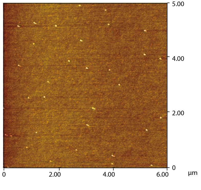
The prevailing cleanroom standard is the Federal Standard 209E which is a document that establishes standard classes of air cleanliness for airborne particulate levels in cleanrooms and clean zones, but there is more and more evidence showing nanoparticles will be the issue presenting an enormous challenge to N10 and N7 production in the semiconductor industry. Particle defects which have a size of less than 20nm were usually detected on the EUV mask[1]. The trend chart and the AFM image of particle defect on the EUV mask are shown in Figure 1 and Figure 2. Besides, nanoparticles are atomic force dominated defects which are difficult to remove, different to the microparticle forces. Within a controlled environment, the concentration of airborne molecular contamination and particles are controlled to specified limits. The level to which these contaminations need to be removed depends upon the manufacture exquisite level required. There are many ways to control contamination of the production, ambient humidity, pressure, temperature, particle filtration, chemical filtration and air flow directions all need to be tightly restricted.
Figure 1. Critical defect trend of EUV mask
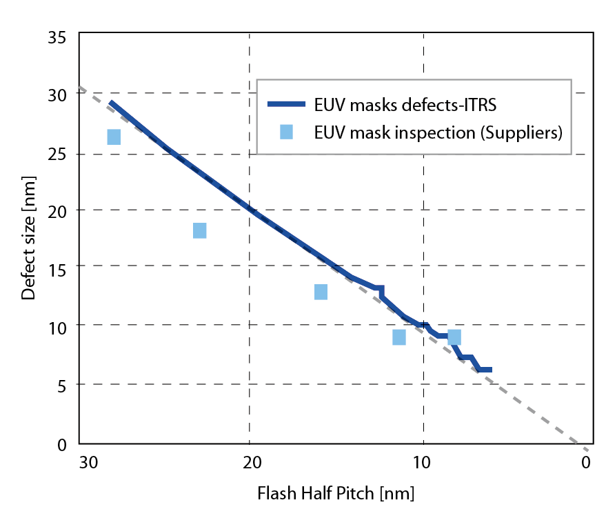
Figure 2. Defects image on EUV mask
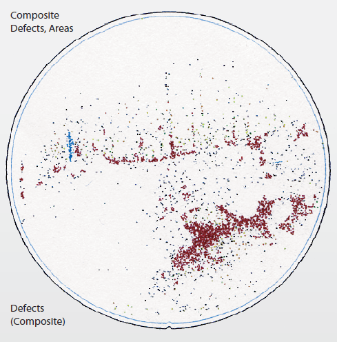
Silicon wafers are used to transfer patterns on the surface of the wafers. The fabrication of semiconductor circuits requires multiple pattern layers, thus anything that is not intended to be deposited on the wafer surface is regarded as defect. For example, the “time-dependent haze” (TDH). TDH is a formation of light point defects which were not present when the bare wafers just left the production line in the manufacturing factory. The “time-dependent haze” is shown in Figure 3.
Figure 3. Wafer light point defects map of time-dependenthaze
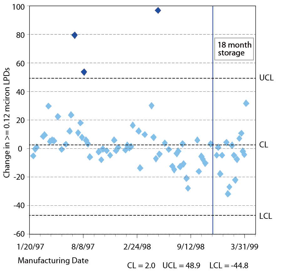
With the application of an AFM image survey, these defects show a random distribution with a localized high density particle region, typically 5-25nm in height and less than 500nm in plane diameter, and these defects could easily be removed by water rinsing or heat treatment. It appears that the time dependent haze may be approximately close to the water spot. The water adsorption on the wafer surface is due to the existence of ambient moisture which is very adhesive to the airborne molecular contaminations. This is the main speculation to the flat dish shape and high hydrosoluble properties of the defects. Larry W. Shive et al. performed a series of wafer storage contamination studies. Dummy wafers were immediately packaged for 6 and 18 months after thorough clean and defect inspection[2]. The trend chart of the wafer defect size larger than 0.12um after 6 month and 18 month storage is shown in Figure 4. It is clear that storage time increment leads no impact to the surface particle numbers.
Figure 4. The trend chart of the wafer defectsize
An accelerated degradation test was also performed. One milliliter water was added into the wafer and then packed into the box. The package was unboxed after 4 hours and 16 hours respectively. The relative humidity was held at a level of about 90%. The main purpose of the accelerated degradation test was to apply water as agent creating extremely high contaminant concentration. Firstly, favor the formation of the water soluble ion. Secondly, assist water soluble organic molecules to be deposited.
The area of a wafer affected by the time dependent haze could be expressed as a function of water volume added to the wafer package shown as Figure 5.
Figure5. The area of a wafer affected by the time dependent haze(TDH) versus water volume

Water adsorption on hydrophilic surface
The adsorption of water on surfaces in ambient conditions is the main phenomena for oxidation, catalysis and lubrication. The adsorption layer of water is on an extremely microscopic scale in dimension. A former study performed a series of water adsorption measurements on a graphite surface, taking nanometer scale images by a commercial SFM with non-contact mode, which could observe the energy dissipation with the distance before the oscillating cantilever tip touched the measuring surface.
These experiments were performed at room temperature; the substrate was exposed to a relative humidity at 90% (RH.). Water adsorption of round and flat island shapes in different diameter were observed.The height of the adsorption layer was about 5nm and the diameters were ranging from 300nm to 600nm shown in Figure 6. The formation of the layers was an evolution from the base layer of 2nm in height and a secondary patch of 5nm layer, shown in Figure 7.
Figure 6. Water adsorption at 90%RH
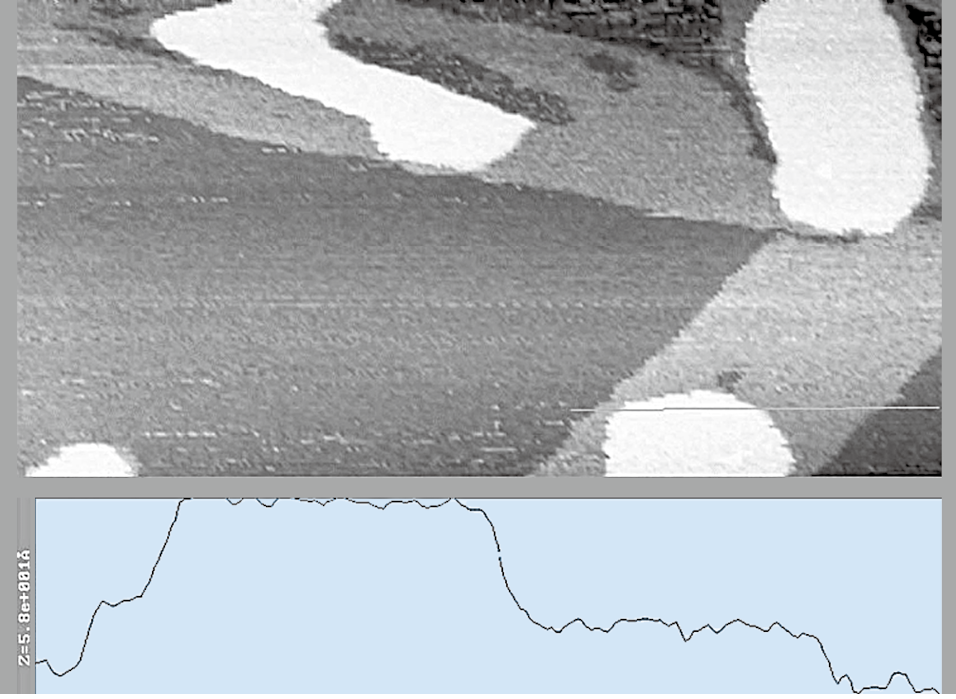
Figure 7. Water adsorption on the graphite surface
 800 nm
When the RH was decreased from 90% to 2%, both the 5nm and 2 nm layers vanished. After all water layers disappeared at low RH, humidified to reverse the process and reaching 90% RH recurrently, those 2nm and 5nm water adsorption layers appeared again.
Different substrate materials for the water adsorption behave diversely.For the surface was flame-annealed gold substrate, inhomogenous water layers were found. At a 35% RH air tight chamber, Au substrate grew a long irregular structure of a water layer 0.2nm in height, which was very approximately to the dimension of the single water molecular. It could be regarded as the first layer of water adsorption on the Au surface.With the increasing of humidity to the level of 65%, the Au substrate is thoroughly covered by the water film.
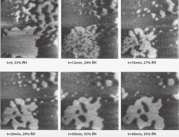
Lei Xu et al. found that, the relationship between the water adsorption area and relative humidity is positive correlated. The increase in humidity will enlarge the water adsorption area. Numerous holes are formed from the inside of the water adsorption layer when the humidity was lowered. All these reduce quantity will recovered by filling the holes and advancing the edges. The water island shrinking and hole formation is shown in Figure 8[4].
Figure 8. SPFM images at different RH (RH was lowed to 24% for an instant and again raised to 35%)
Water adsorption on hydrophobic surface
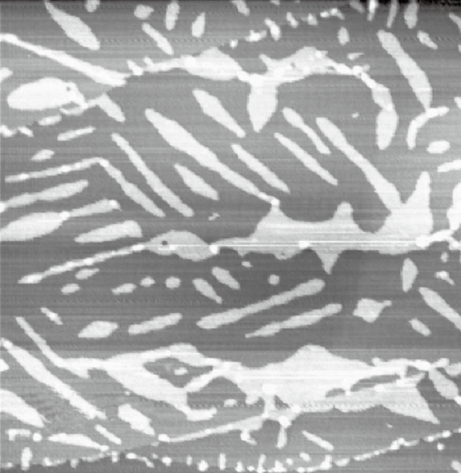
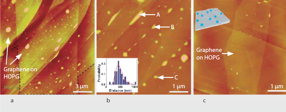
The interaction of water vapor with hydrophobic surfaces is very interesting. The adsorbed water on the hydrophobic surface was similar to the hydrophilic surface.For the hydrophobic surfaces, the attraction force between the water molecular and the surface is much weak than the force between the water molecular itself. Therefore, no macroscopic water droplets of water could be adsorbed on the hydrophobic surface. Water will evaporate before the formation of macrodroplets have been completed.A recent study found that, the total adsorbed water on a wax-coated highly hydrophobic glass surface was unexpectedly more than the water on hydrophilic glass surface[5].Conjecture to this phenomenon is that water adsorbed on the highly hydrophobic glass surface in the form of microdroplets. These microdroplets are nanometer size ranging from 10nm to 100nm in average. According to atomic scale surface scanning by the atomic force microscope (AFM), the occurance of microscopic water droplets is at the surface defect, like porous and step-edges, shown in Figure 9. And Figure 10 shows AFM topographic images of graphene covering HOPG surfaces under ambient conditions (~40% RH). Distribution of the microscopic water droplets was aligned along the step edges, the length is around 450 nm. Without complications, in the controlled variant experiments at different RH, the number density and sizes of the water droplets on a hydrophobic surface were reduced with the descending humidity.
Figure 9. Microscopic water droplets at step-edges
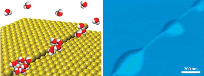
Figure 10. AFM topographic images at different RH
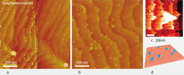
On the hydrophobic graphite surfaces which is about 90° contacting angle with water, at the step edges of graphite, there were water droplets nucleated at the edge ranging from 5~15nm in height found. The dimension of the graphite step edge is 0.335nm, which is far below the size of the water droplet. It’s interesting that, integrating the height of water layer on the surface, helped to discover thathydrophobic surfaces have more water adsorbed on the surface than the hydrophilic surfaces do. For the measurement on surface with controlled condition of humidity at 40%, there are 73% of the areas which are occupied by the water adsorbed mono layer on the graphite surface of hydrophobic property, by contrast, there are only 45% of the water adsorbed monolayer on the mica of hydrophilic surfaces.
Similar to the appearance of edge nucleation, the atomic scale defect on the surfaces is also competent to nucleate water droplets. The adsorbed water droplet at surface defect showed a much larger dimension than the defect size. For example, concave etch pits will become convex appearance made of adsorbed water droplets. The AFM topographic image is shown in Figure 11, AFM topographic image of graphene covering H-terminated Si(111) surface under ambient conditions (~40% RH) and a schematic showing that water nanodroplets (blue) reside along edges and at etch pits.
Figure 11. Water adsorption on H-terminated Si(111) surface.
The influence of humidity
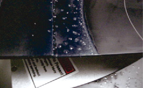
The crucial challenges of micro-contamination control in next generation semiconductor factories are still airborne molecular contamination (AMC). Condense defect is one of the most challenging problem to be confronted with [6]. The image of the defect is shown in Figure12[7]. Yiting et al. found that the actions of FOUP N2 purge can impede the degradation of the wafer surface, prohibiting the formation of condense defect and corrosion defect effectively. There are two major types of purge gas used for this purpose. Ultra-pure air[9] and nitrogen gas, both gases offer a highly controlled particle contamination, organic inorganic contamination and humidity. Regards to site applications, purging FOUP is prevailing. There are many kinds of purging systems, like overhead buffer continuous (OHC) N2 purge charging system, standalone N2 purge charging system, embedded stocker N2 purge charging system and overhead buffer (OHB) N2 purge charging system. The common ground of nitrogen gas and Ultra-pure air is that they both offer low relative humidity environment. This is the main method how purging systems suppress the wide range damage mechanism of different volatility level compound. All these defect occurrences start from the water adsorption on the wafer surface.
Figure 12. Condense defects found inpost poly-silicon etching

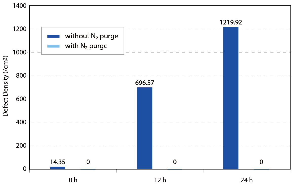
According to the former researches, the behavior of water adsorption form film or island on the wafer surface is known. Howard Tsao et al. performed a series of FOUP environment control and condense reduction experiments. Purified nitrogen gas was offered as high quality AMC free and extremely low humidity purging source for verification the assumption. The result indicated that the FOUP surface and wafer surface will adsorb the vaporization of chemicals and lead to corrosion defect and condense defect. The N2 purge system obviously suppressed the formation of defect in crucial processes like post AlCu metal line etching processes, post poly-silicon etching and post implantation. Condense defect performance with and without N2 purge in different processand queue time is shown in Figure 13~15.
Figure 13. Condense defect performance w/ andw/o N2 purge in different process after 24h queue time
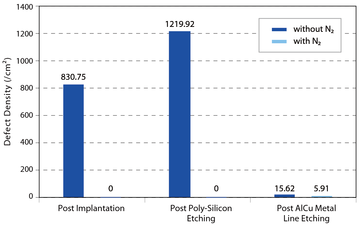
Figure 14. Post implantation layer condense defectperformance with and without N2 purge in different queue time.
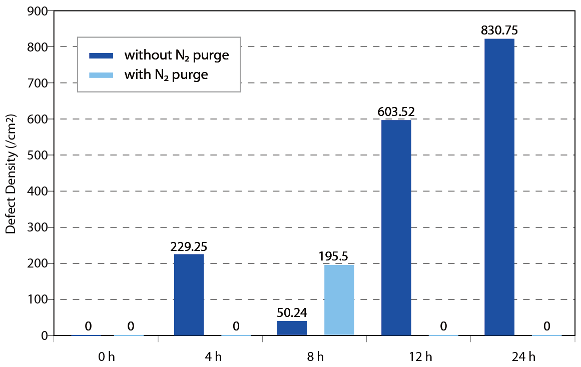
Figure 15. Post poly-silicon etching condense defectperformance with and without N2 purge in different queue time.
Minienvironment enclosure is used to offer class 1 production environment. HEPA filtration module provides particle free vertical laminar airflow. But particle pollution is still a problem occurring in the isolated booth. For many reasons one could believe that the particle is formed from the inside of minienvironment enclosure. To address this problem, a combination of particle active sampling of aerosol condensation particle counter and passive sampling of wafer substrate was performed. Ion chromatography sampling was utilized to measure AMC concentration in the booth.
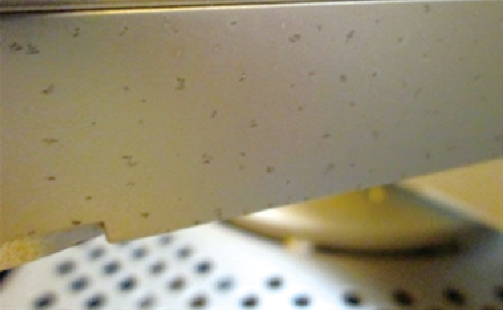
White powder like rust was observed at the surface of robot and hatch, which is shown in Figure 16.
Figure 16. White powder like rust on the robot
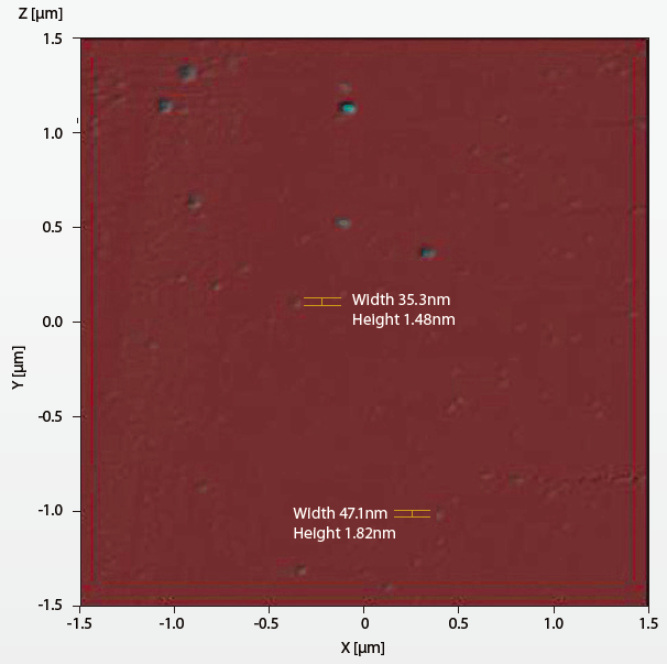
Active sampling of the aerosol condensation particle counter accumulated the counts of particles which were larger than 10nm, the measuring log showed extremely low particle concentration in the minienvironment enclosure. Passive sampling of the wafer substrate were sent to take scanning electron microscopy (SEM) images, resulted blurred image of particle clusters, the SEM image is shown in Figure 17. The nanoparticles were found on the wafer substrate forming vague images due to the shallow depth of field. For the resolution limit of Z axis is about 10nm in scanning electron microscopy apparatus.The wafer substrate was finally sent to take AFM measuring the particles on the surface. The result of the AFM survey found that the particles were disk like in shape. The heights were less than 2nm and the diameters were ranging from 20nm to 80nm. The AFM image is shown in Figure 18. The ion chromatography sampling exhibited high chloride ion and ammonium ion concentration in the samples taken. The AMC concentration inside the mini-environment was an incredible amount higher than the cleanroom environment.
Figure 17. SEM images of nanoparticles
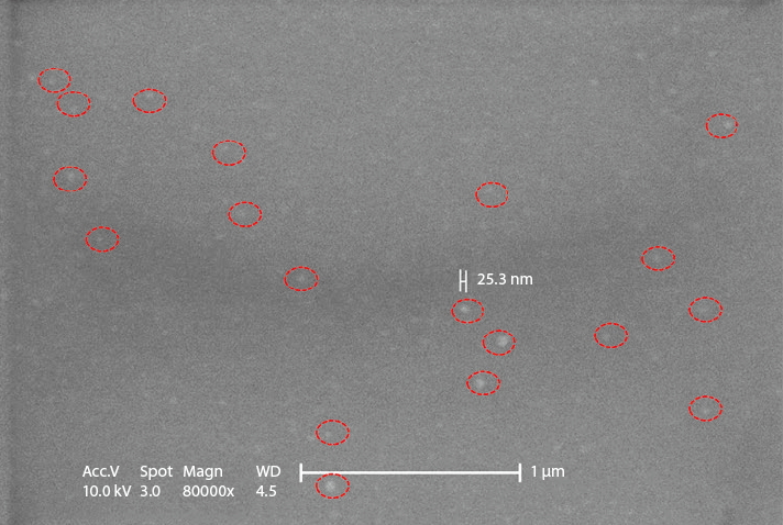
Figure 18. AFM images of nanoparticles
Result and discussion
This article summarizes recent efforts to explore the benefits of low humidity in FOUP purging systems. Former studies revealed the impact of the existing humidity in the semiconductor manufacturing factory and described the efficiency improvement in suppressing the defect formation. Several measurements were performed involving Ion chromatography, aerosol particle counter, SEM and AFM. The results show that the particle defects are formed from the inside of mini environment rather than the outside air. ITRS assumed these nanoparticles are defects in spherical shape. For which is likely to be referred to as the chemical reaction product, rather than the debris of irregular appearance. Furthermore, nanoparticles should be highly suspected of the acid-base neutralization product, that’s why the reduction of humidity in the cleanroom ambient will result in the yield enhancement. The existence of water film on the surface will contribute to the formation of positive and negative ions. Ions are highly reactive causing corrosion and oxidation reactions. The idea behind the survey of nanoparticle defects offers a brand new way to recognize a novel cleanroom design for the next generation of semiconductor fabrication.
參考文獻
- Michael Lercel,Solving the nanodefectivity problem, SEMATECH,November 2012
- Larry W. Shive, Richard Blank and Karen Lamb,Investigating the Formation of Time-Dependent Haze onStored Wafers,Micro Magazine,2001
- M. Odelius, M. Bernasconi, M. Parrinello,Two Dimensional Ice Adsorbed on Mica Surface,Physical Review Letters,78,2855,1997.
- Lei Xu, Anna Lio, Jun Hu, D. Frank Ogletree, and MiquelSalmeron,Wetting and Capillary Phenomena of Water on Mica,The Journal of Physical Chemistry B, 1998, 102, 540-548
- Peigen Cao, KeXu,Joseph O. Varghese, and James R. Heath,The Microscopic Structure of Adsorbed Water on HydrophobicSurfaces under Ambient Conditions,Nano Letters,2011
U. Baltenspergera. Real-time characterization of ultrafine and accumulation mode particles in ambient combustion aerosols.Journal of aerosol science 33 (2002) 1139–1154. - Shou-Nan Li1, Hui-Ya Shih, Shaw-Yi Yen, Jean Yang, Case Study of Micro-Contamination Control,Aerosol and Air Quality Research, Vol. 7, No. 3, pp. 432-442, 2007.
- YitingKuo, Howard Tsao, TuungLuoh, Ling-WuYang, Tahone Yang, Kuang-Chao Chen, andChih-Yuan Lu, "FOUP Environment Control andCondense Reduction", e-Manufacturing & DesignCollaboration Symposium 2012.
- Tzu-Sou Chuang, Luh-Maan Chang, To Mitigate Airborne Molecular Contamination Through Ultra-pure Air System,Building and Environment, Vol 59, January 2013, pp 153-163.
留言(0)